Abstract
The UCLID (University College London Implantable Device) wearable
speech processor has been designed to provide as much computational
power and flexibility as possible so as to support research into
speech processing algorithms for cochlear implants. The stimulator
circuit contains a separate current generator for each electrode.
The current generators use a novel circuit configuration constructed
from standard components to give very high performance.
1. Introduction
The UCLID project requires a speech processor for use with a multi-channel,
percutaneously connected intracochlear implant. The rationale
behind the design was to be able to implement the widest possible
range of speech processing strategies. Two commonly used strategies
are compressed analogue (CA) and continuous interleaved sampling
(CIS) (Wilson et al, 1991). These strategies make different demands
on the hardware both in terms of signal processing and electrical
specification. In particular, CIS requires fast rise and fall-time
pulses of relatively high amplitude and short duration (10-200µs/phase)
while CA requires the generation of arbitrary waveforms at lower
amplitudes.
This paper describes the design of the current generators used in the UCLID processor. Modelling of the digital to analogue converter (DAC) configurations was done using the SPICE electronic circuit simulation software (see appendix A for a listing of the SPICE circuit descriptions and associated batch and perl scripts used to generate them).
The specification of the current generators was as follows.
Figure 1B shows a ground referenced current generator which allows multi-channel operation. However, this circuit requires extremely well matched components and a high slew-rate opamp. Opamps require a high operating current in order to get fast slew rates and are unsuitable for use in a low power system. A further drawback is that the output of the DAC has to go both positive and negative. If the DAC has any non-linearity then the outputs for the positive and negative pulses will not be equal.
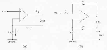
Figure 1. Voltage to current converters.
3. Current-controlled current generator
An alternative is not to use a voltage-controlled current generator
but instead to use a current output DAC and a pair of current
buffers (for positive and negative pulses). This removes the
need for fast op amps in the signal path giving fast rise times
and low power consumption. Since most DACs are inherently current
mode devices, this is a natural and efficient mode of operation.
In order to ensure equal positive and negative pulses the current buffers must be well matched. The use of a matched pair or a single device with twin current buffers is needed. The 3080A operational transconductance amplifier (OTA) can be used in this way.
Figure 2 shows a schematic of a typical R-2R DAC connected to an OTA. The polarity of the differential voltage across the + and - inputs selects a positive or negative current flow through the load. The magnitude of the output current is set by the current flowing into the IIN pin from the DAC. This magnitude and polarity scheme also eliminates the problems associated with any DAC non-linearity.
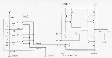
Figure 2. Schematic of a typical R-2R DAC connected to an OTA
This system works well (fast response, low power etc) but fails to meet the DNL spec (Figure 3). To quantify the DNL the following steps were taken.
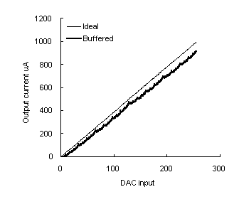
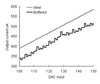
Figure 3. DNL error caused by current buffer (detail on right).
For Figure 3 the average DNL was 2.6, worst case was 5.4.
The DNL is due to an imbalance in the DAC resistor ladder since one of the DAC outputs is not at ground potential but at the potential of the OTA IIN pin. The potential at this point is that created by the base-emitter junction of the OTA input transistor. This voltage increases from approximately 600mV to 800mV as the current increases from 1µA to 1mA.
To reduce the DNL, the ends of the resistor ladder need to be at the same potential. This can be achieved using an op amp as a unity gain buffer to drive the second IOUT pin with the potential at the first IOUT pin. This gives a more regular pattern to the DNL but does not significantly reduce the DNL figures.
To ensure the DNL is within acceptable limits the tail of the resistor ladder (the AGRND pin on most DAC chips) also needs to be at the same potential as the IOUT pins. This circuit configuration (Figure 4) produces the input-output function shown in Figure 5. The slope of the input-output function is not identical, since the reference voltage is reduced by a diode drop, but the change in gain can be compensated for elsewhere. The DNL in this case is 0.019 bits worst case, 0.012 bits average.
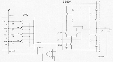
Figure 4. Modified DAC configuration to remove DNL
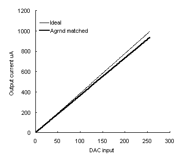
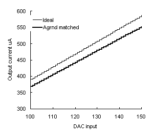
Figure 5. Input-output function for modified DAC configuration (detail on right).
Since the potential at the IOUT pin is only one diode drop, the opamp needs only modest output slew rate (1V/7#181sec). Further modelling using SPICE predicts that to degrade DNL performance by less than 0.1bits the input offset voltage needs to be <500V. There are many devices that meet these specifications with power supply current less than about 1mA.
4. Summary
The use of a current output DAC combined with an OTA and a few
other components produces an accurate, fast current generator
ideally suited to a research-based cochlear implant speech processor.
Acknowledgements
This work was supported by the Worshipful Company of Clothworkers
and Defeating Deafness (The Hearing Research Trust).
References
Wilson B., Finley C., Lawson D., Wolford R., Eddington D. and
Rabinowitz W. (1991) Nature, 353:236-238
Appendix A SPICE models
A separate SPICE model was used for each circuit configuration. The following is the file (DAC5.CIR) for the configuration shown in Figure 4 (the configuration used in the UCLID device.
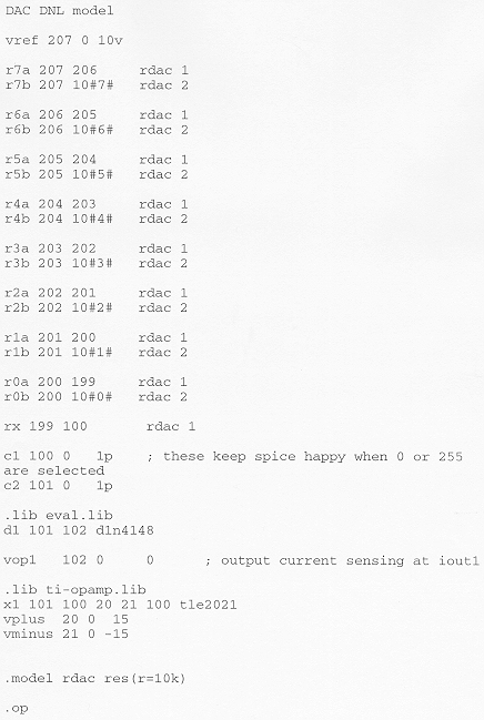
A perl script (MKCIR.PL) was used to convert the text between the #s to either 0 or 1. This allows simulation of the steady state for any input code.
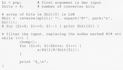
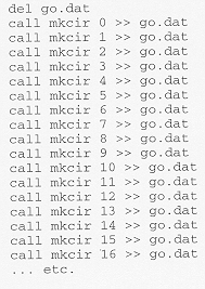
A batch file (MKCIR.BAT) was used to run the SPICE simulation and extract the output current for any input.
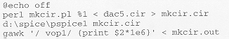
A second batch file can then be used to generate a data file for a ramp input.
© Julian Daley and John R. Walliker.